
Link Switch-HP Design parameters
Hello,
I am using Link switch-HP (LNK67xxE) for 10-35W flyback converter designs. We have multiple designs with different input voltage ranges and output power level. Designs are generated using PI Expert & PI Xls , these designs are working fine with some iterations of feedback and programming resistors values.
However, I need better understanding of the parameters used in design sheet. Can you clear the following points for me-
1) Is it possible to generate a design having multiple outputs with different ground reference?
2) What is the output capacitor formula being used in PI Expert design sheet?
3) If my input voltage range is 80V-300V (DC), then can I make the Link Switch turn off below 80V and above 300V?
I am attaching one of the design sheets for 80-300 Vdc. Please have a look and suggest if the design is already optimized or I can do better based on design specifications.
Quick response would be appreciated.
Thanks,
Jasvant Singh
Files
| Attachment | Size |
|---|---|
| LNK6763E_15W.pdf | 1.6 MB |
Comments
Hello,
Thank you for the reply. Please find the design specifications for the SMPS which is currently under testing.
Input voltage - 150 to 510 V (DC)
Output 1 - 24V, 250mA
Output 2 - 15V, 500mA
Output 3 - 8V, 200mA
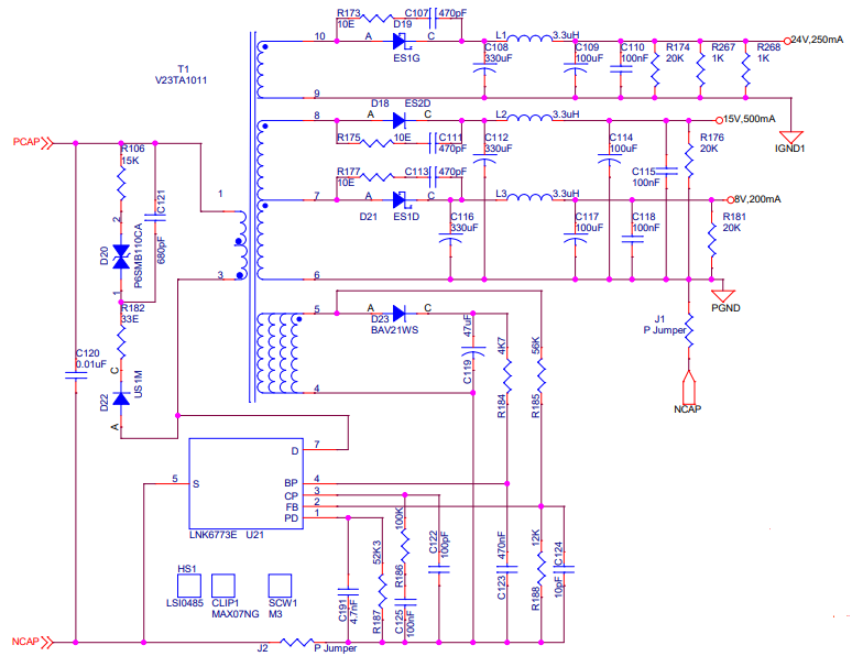
Output 2 & output 3 have the common ground but 24V ground is isolated.
I am also attaching the design sheet and schematic.
Also, currently we are facing a problem regarding output voltage dipping when we load the SMPS (designed using LNK6773E). I am also attaching output voltage waveform.
In waveform, Ch1—15V output. [@Vin = 320 V (DC)]
| Attachment | Size |
|---|---|
| Design sheet (PI xls) | 1.62 MB |
| SMPS schematic | 119.54 KB |
| output voltage waveform (15V) | 1.27 MB |
Hi Jasvant Singh,
We have reviewed the PIExpert.
Good thing that you have stack the 15V and 8V winding. This will help in the regulation.
Please see attachment. It contains suggested TRF construction. And, it also contains information that Bias winding should be stable during sampling time 1.2us - 2.5us.
I suggest also to use the 15V in the PIExpert instead of the 24V. 15V have the highest output power.
Please also follow the recommended lay out in the datasheet.
Thanks
Regards
PI CHLOE
| Attachment | Size |
|---|---|
| Suggestions.png | 86.32 KB |
Hello,
Thank you for the response, appreciate it. We were using the same transformer construction as you suggested. From next time, we will use the highest power output as main output as you suggested.
Regarding the ringing in VDS (if it is there), we have to use better snubber circuit. Please let me know if my understanding is correct.
The output voltage dipping problem got solved when we added 4.7nF as Cpd in parallel of programming resistor. Is using Cpd mandatory? If not, then in which cases it is required?
Also, I have not got any answer regarding the output capacitor formula being used in PIExpert which was one of the first questions I asked in this ongoing thread.
Regards,
Jasvant Singh
Hi Jasvant Singh,
Your understanding is correct. If there are ringing during sampling of the feedback, need to improve the snubber circuit.
Cpd also works as a noise filter capacitor for the PROGRAM pin, it is recommended add Cpd capacitor.
Looking the PIExpert for LNK HP, there is no output capacitor field. LNK HP Application Notes contains information on the selection of output capacitor.
Thanks
Regards
PI-Chloe
Hello,
Thank you for the response. First two points are clear regarding the Snubber and Cpd.
However, regarding the output capacitor LNK HP application notes only talks about ripple current rating of the capacitor (also temperature, life span). But what about the actual value of the capacitor(uF)?
If the value of the capacitor is not important then why PIExpert generates different capacitor values for different outputs.
Please clear this point for me.
Regards,
Jasvant Singh
Hi Jasvant,
The application note talks about how the output capacitor can be picked. To start, you need satisfy two things:
1. The ripple rating of your chosen output capacitor must be greater than the calculated output ripple current from the spreadsheet.
2. The voltage rating of your chosen output capacitor must be greater than or equal to 1.25 x Output Voltage
These two conditions are the reason why different capacitor values are chosen for the different outputs of your design. Since you have different output voltages, it would make sense that the capacitors chosen for each differ.
By extension, you could just pick one capacitor value for all your outputs as long as it satisfies the conditions above for each of the output. However, if you want to optimize your design, you can pick the smallest value capacitor that satisfies the condition for each output.
To summarize, the current and voltage rating of your chosen output capacitor should take precedence over the capacitor value itself.
Thanks and Regards,
PI - Pompeii
Hello,
Thank you for the response. I understand that we have to satisfy voltage and current rating criteria as you have explained above.
But peak to peak voltage ripple will depend on the capacitor value, right?
If the ripple is anyway low for Link switch-HP controller due to high switching frequency (my assumption), Then do we need to consider capacitor value(uF) for lower switching frequency controllers? and what would be typical value of that switching frequency?
And what formula we need to use for calculating capacitance in that case?
Please give your inputs on the above points.
Thanks,
Jasvant
Hi Jasvant,
To give you a high-level overview, you may consider the formula:
C = I / (2 * fs * Vpp)
Wherein:
C - output cap value
I - load current
fs - switching frequency
Vpp - peak to peak voltage ripple
You can use this to check the minimum output capacitor value you need to contain your voltage ripple to a certain level. However, a good rule of thumb would be to use around 10uF per watt of your output. You can adjust that to get a larger or smaller capacitor upon evaluating your design in the bench or simulation. You just have to make sure that you satisfy the rating requirements previously discussed.
As for the switching frequency, I cannot tell you an exact value but that should usually be in the order of tens of kHz.
Thank you.
Regards,
PI - Pompeii
Hello,
Thanks for the reply.
A) Can you please share the units of the parameters being used in above formula?
B) If we use your formula for Cout or take thumb rule 10uF/W, why it is not working for any of the reference design provided by PI.
For example, let's take DER-882
Load current = 1.25A
Switching frequency = 132 kHz
Vpp = 120 mV
Cout should be 39.45uF (based on your formula).
Or if we follow 10uF/W rule then it should be 150uF. (Po = 15W)
But the value being used is 680uF + 100uF in ref design. Why there is so much difference between calculated and used value.
And this is true for all the reference design provided by PI for Link-switch HP.
Kindly provide more clarity on this.
Regards,
Jasvant Singh
Hi,
A) The units of the parameters for the formula are SI Units ( F, A, Hz, V ).
B) As I mentioned, the formula will give you the minimum capacitance value which might work. You still have to evaluate the design using a simulation or at the bench to determine whether it meets your specifications and decide to increase the capacitor from there.
It is the same case for the rule of thumb mentioned. It is simply a starting point from which you will evaluate the design, instead of starting at the minimum capacitance value. The capacitor may be increased based on the measured temperature rise under the worst-case load and ambient temperature conditions.
For the capacitor values used in the reference designs, those have undergone evaluation already and the values have been adjusted based on the measurements from the bench. The used capacitance should definitely be higher than the minimum capacitance calculated. By how much, that depends on the evaluation of the circuit.
You have multiple options for your design, you can pick a reference design close to your application and follow the components from there. But I would recommend you use the PI Expert tool itself; it does the simulations for you and picks the components based on those simulations. You don't have to iterate through multiple capacitor values for your specification because the tool will do that for you already.
Regards,
PI - Pompeii
Dear Pompeii,
Thanks for your support during our SMPS design process.
Currently, we are testing the board over the entire input voltage range with varying the load%. We are facing SMPS auto-restart problem when we turn-on the SMPS at Higher Vin with 90-100% load.
If we turn-on the load after turning on the SMPS, then there is no problem. But if load is already at 90-100% and we turn-on the board at Vin > = 280V, then board goes into restarting mode.
I am attaching our design sheet (PIxls), Schematic and one PDF document containing problem details and test waveforms.
PDF document contains CP pin waveform in normal & faulty conditions and VDS, IDS waveform at different conditions. Please have a look and clarify the points asked in the document.
Since we are in middle of the product testing, please consider it as very urgent and get back quickly.
Design specifications:
Po = 15.1W,
V0(1,2,3) = 15V, 8V, 24V [24V output is w.r.t. isolated ground]
Vin (range) = 110-510V
| Attachment | Size |
|---|---|
| Schematic | 96.34 KB |
| Design Sheet | 202.93 KB |
| Problems and test waveforms | 520.33 KB |
Hi jasvant007
Please see attach word file for the observation on Ids and Vds waveforms.
For the IDS, it seems that there is a set up concern. We can discuss this by showing to use where did you cut the trace for current probe.
For the start up concern, can you send us the waveforms of the output voltage. how high does the Vo reach during start up.
Thanks
Regards
PI-Chloe
| Attachment | Size |
|---|---|
| forum jasvant007.pdf | 414.24 KB |
Hello Chloe,
Thanks for the response. We will cross-check the trace-cut for the Ids waveform once again.
If the TRF is operating in discontinues mode, is that a problem?
Regarding start-up problem, please find the attached document containing output voltage and current waveforms at start-up.
| Attachment | Size |
|---|---|
| Output voltage and current waveforms.pdf | 407.18 KB |
Hi jasvant007
There are two operating modes of SMPS. These are continuous mode and discontinuous mode. In discontinuous mode, all energy of the transformer is transferred to the output. You can observe this when the IDS slope starts to ramp- up at 0A.
For the startup, can you check if the PSU will start up properly if we increase the Rpd resistor. It seems to me that at start up the energy is not enough to push the output to its regulation point. Increasing Rpd will increase the ILIM.
I think you are using 52.3Kohms. Please check if you use 78.7kohms.
Thanks
Regards
Patrick
Hi,
I have checked even with 100% current limit i.e., 124K Rpd resistor. The problem is still there.
Can you please check figure no. 27 & 28 from Link switch-hp datasheet; I think allowable drain current drastically comes down as drain voltage goes past 500V.
- Is that creating a problem at higher input voltages? Please provide your POV.
- There is sharp spike in output voltage at start-up at higher input voltages, why so and how to resolve this? [ for ex- 15V output goes up to 19V then settles at 15V]
-
We have multiple designs based on Link switch-hp and in most designs, only during certain input voltage ranges, output voltage ripple (disturbance/noise) increases while output voltage is neat & clean for entire input voltage range except those particular small ranges.
Example for 3rd point -- Input voltage range = 200 to 800 Vdc [another FET stacked with Link switch]
output voltage ripple increases - a) from 340 to 380V.
b) from 650 to 700V
other than a and b input ranges, output is stable and having negligible(design) ripple for Vin = 200V to 800V.
Thanks,
Jasvant
Hi jasvant007
Datasheet figure 27 and 28 are the safe operating area (SOA) of the FET. It will not stop the IC to operate or shutdown during start up.
I think the major difference from other design that you are mentioning is this is a multiple output flyback. As I said in the first thread of this question, Multiple output design of LNK HP is possible but complicated because IC is a primary side regulation. Meaning, it indirectly sense the output voltage via the bias winding. this will have a poor cross regulation response.
Now concern is that it cannot start up at high line loaded.
During start up: If VO cannot reach regulation within a specific time it will go to AR. I think this time is around 75ms. I have this idea looking to your waveforms of Output rise time. We suggested to increase the Rpd to increase ILIM. Increasing ILIM will help to speed up the rise in the output voltages. but this not work. another thing that we can look to is the output voltage capacitance of each output. the higher the capacitance will make the output rise time slower.
Please try to reduce the output cap. Please try to monitor all output at the same time to determine the effects of each iteration. At this point we need to check if this causes the issues at high input start up.
If this solves the start up concern, need to assess the value of output capacitors if the output ripple is still tolerable.
Thanks
Regards
PI-Chloe
Hi Jasvant Singh,
Good Day!
Thanks for using Power Integration products.
Yes, it is possible to design a multiple output with different ground.
But there is a concern because the output is regulated by indirect sensing method or PSR (Primary Side Regulation).
Meaning cross regulation between output will be not that good.
Please help to provide your design specification so that we can answer your inquiry properly.
Input Voltage:
Output_1 Voltage and Current
Output_2 Voltage and Current
Output_n Voltage and Current
Thanks
Regards
PI-Chloe